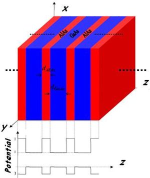
In semiconductor physics , the term superlattice is understood to mean a solid-state structure in which, in addition to the periodic potential of the crystal lattice, there is an additional potential whose period substantially exceeds the lattice constant [1] .
The following types of superlattices are distinguished:
- Composite superlattices are epitaxially grown periodically alternating thin layers of semiconductors with different bandgaps [2] .
- Doped superlattices - a periodic potential is formed by alternating ultrathin layers of n- and p-types of semiconductor, which are separated from each other by undoped layers [3] .
- Spin superlattices - formed by periodic alternation of layers of the same semiconductor. Some layers are doped with non-magnetic impurities, while others are magnetic. Without a magnetic field, the energy gap in the entire superlattice is constant, a periodic potential arises when a magnetic field is applied [4] .
- Superlattices formed in a two-dimensional electron layer (for example, in a MIS system: metal-dielectric-semiconductor) by periodically modulating the surface charge plane.
- Superlattices, the potential in which is created by periodic deformation of the sample in the field of a powerful ultrasonic or standing light wave.
Along with semiconductor superlattices, there are also magnetic superlattices and ferroelectric superlattices. The pioneers of solid-state superlattices are Tsu and Esaki .
In microelectronics, superlattices are used to create generator, amplification, and converter devices in the millimeter and submillimeter wavelength ranges. The transition to the use of elements of microelectronics based on superlattices is necessary when the size of the elements is less than 0.3 microns, when traditional transistor structures will be inoperative due to fundamental physical limitations [5] .
Notes
- ↑ Buzaneva, 1990 , p. 203-241.
- ↑ Buzaneva, 1990 , p. 205-209.
- ↑ Buzaneva, 1990 , p. 210-213.
- ↑ Buzaneva, 1990 , p. 231-233.
- ↑ Buzaneva, 1990 , p. 235-241.
See also
- Bloch Oscillations
- Multiple quantum well structures
Literature
- R. Tsu and L. Esaki. Tunneling in a finite superlattice (neopr.) // Applied Physics Letters . - 1973.- T. 22 . - S. 562 . - DOI : 10.1063 / 1.1654509 .
- Buzaneva E.V. Microstructures of integrated electronics. - M .: Radio and communications, 1990. - 304 p.